Türkçe

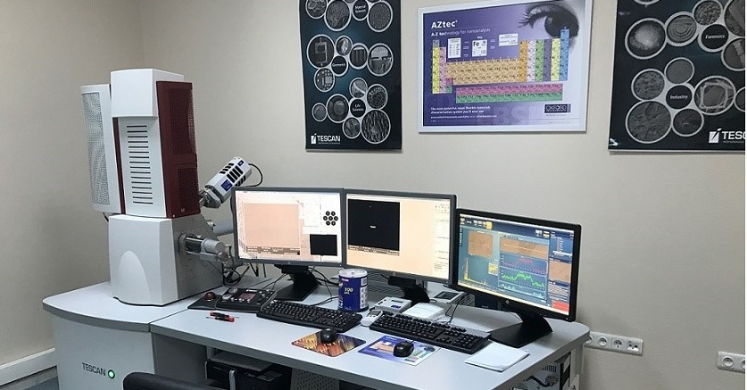
Scanning Electron Microscope (SEM)

Scanning Electron Microscope (SEM) / Device: TESCAN MAIA3
Introduction:
The TESCAN MAIA3 is an ultra-high resolution SEM with excellent imaging capabilities in the whole range of beam energies. A versatile detection system and high spatial resolution allows the observation of even the finest surface details. This is an essential feature for comprehensive characterization of nanomaterials, for observation of beam-sensitive samples common in the semiconductor industry and for comfortable imaging of non-conductive samples including uncoated biological specimens.
Specifications / Applications:
Five-axis eccentric stage can accommodate a specimen of up to 4-inch in diameter.
Imaging up to 1,000,000X, backscattered electron (BSE), X-ray analysis of elements down to carbon with energy dispersive X-ray spectroscopy (EDX) detector and Electron Backscatter Diffraction (EBSD) analysis.
The extended low-vacuum mode allows imaging on non-conductive samples including biological specimens.
Fotoğraflar